Archive | REF: E3565 V1

Digital Signal Processors (DSP)

Authors: Gérard BLANCHET, Patrick DEVRIENDT

Publication date: February 10, 2000 | Lire en français

You do not have access to this resource.
Click here to request your free trial access!

Already subscribed? Log in!

Automatically translated using artificial intelligence technology (Note that only the original version is binding) > find out more.

    A  |  A

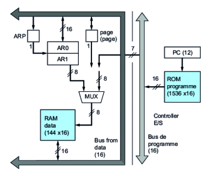
    2. DSP memory architecture

    It's a commonplace to say that memory is "the" bottleneck in processor operation. Many tricks can be used to achieve a throughput compatible with the processor's speed: caches, organization into banks and burst access, multi-access memory, etc. [2] .

    .Simplified diagram of the TMS32010 memory architecture
    You do not have access to this resource.

    Exclusive to subscribers. 97% yet to be discovered!

    You do not have access to this resource.
    Click here to request your free trial access!

    Already subscribed? Log in!


    The Ultimate Scientific and Technical Reference

    A Comprehensive Knowledge Base, with over 1,200 authors and 100 scientific advisors
    + More than 10,000 articles and 1,000 how-to sheets, over 800 new or updated articles every year
    From design to prototyping, right through to industrialization, the reference for securing the development of your industrial projects

    This article is included in

    Electronics

    This offer includes:

    Knowledge Base

    Updated and enriched with articles validated by our scientific committees

    Services

    A set of exclusive tools to complement the resources

    Practical Path

    Operational and didactic, to guarantee the acquisition of transversal skills

    Doc & Quiz

    Interactive articles with quizzes, for constructive reading

    Subscribe now!

    Ongoing reading
    DSP memory architecture